Supramolecular engineering on wide-bandgap semiconductors
On-surface reactions provide a general means for constructing defined molecular nanosystems with novel properties. Wide-bandgap semiconductors offer a platform to prevent the quenching of electronic and optical excitations. Our scientific purpose is thus focused on exploring the potential of GaN and TiO2 single crystals as well as Cu2N thin films for on-surface reactions.

Focus Group: Molecular Assemblies and Covalent Nanostructures on Wide-Bandgap Semiconductor Surfaces
Prof. Lifeng Chi (Soochow University), Alumna Hans Fischer Senior Fellow | Mohammadreza Rostami (TUM), Doctoral Candidate | Hosts: Prof. Johannes Barth, Prof. Martin Stutzmann (TUM)
Gallium nitride (GaN)
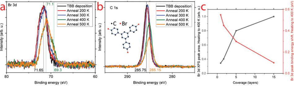
GaN, a wide-bandgap semiconductor with absorption and emission in the ultraviolet/visible range, is proposed as an alternative to metallic surfaces for assembling organic molecular structures intended for optoelectronic applications. However, the formation of a persistent surface oxide layer in air considerably limits the use of GaN for well-defined interfaces. We have investigated, characterized, and processed n-type free-standing c-plane hexagonal wurtzite GaN crystals (Fig. 1a) grown by the hydride vapor phase epitaxy and ammonothermal growth methods. Surface cleaning and full removal of the oxide layer on GaN surfaces could be reproducibly achieved via sputtering and annealing cycles, as evidenced by X-ray photoelectron spectroscopy (XPS) and low-energy electron diffraction (LEED). Scanning tunneling microscopy (STM), however, indicated substantial roughening of the GaN surface and the formation of unwanted Ga-rich islands and clusters. Although ammonia (NH3) and bromine (Br) treatments compensated the N / Ga atoms ratio reduced by sputtering (Fig. 1b), the surface morphology remained rough, exhibiting randomly shaped and distributed hillocks. Nevertheless, by introducing 1,3,5-tris(4-bromophenyl) benzene on GaN (Fig. 2), on-surface debromination and polymerization of the molecules upon heating GaN (Fig. 2) and the removal of Ga atoms by Br atoms during the desorption were observed and proven by XPS studies [1].
Figure 1
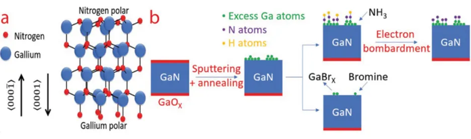
Figure 2
Titanium dioxide (TiO2)
Although on-surface synthesis provides promising strategies to successfully construct various graphene nanoribbons (GNRs) with precise width control, the use of metal surfaces typically involves the quenching of electronic and optical excitations, thus preventing the study of intrinsic electronic structures and resulting in contradictory reports. Semiconducting titanium dioxide (TiO2) including rutile TiO2 (110) and anatase TiO2 (101) surfaces can be used for photocatalysis of surface-assisted Ullmann coupling. We first systematically studied the influence of light and Fe adatoms on the debromination of 4,4”-dibromo-p-terphenyl precursors affording poly(para-phenylene (PPP as the narrowest GNR) wires through the Ullmann coupling reaction on a rutile TiO2(110) surface by STM and XPS. The temperature threshold for bromine bond cleavage and desorption is reduced upon exposure to UV light (240-395 nm wavelength), but the reaction yield could not be improved. However, in the presence of co-deposited Fe adatoms, precursor debromination occurred even at 77 K, allowing for Ullmann coupling and PPP wire formation at 300-400 K, i.e., at markedly lower temperatures compared to the conditions without Fe adatoms. Furthermore, scanning tunneling spectroscopy data revealed that adsorbed PPP wires feature a HOMO-LUMO gap of ≈ 3.1 eV. [2]. By employing PPP wires with extended length single-molecule conductivity, measurements become possible by lifting the wire using an STM tip, as we demonstrated in related experiments [3].
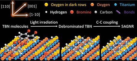
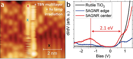
We furthermore prepared 5AGNRs on semiconducting rutile TiO2 (110) and anatase TiO2 (101) surfaces using photocatalysis of surface-assisted Ullmann coupling of 1,4,5,8-tetrabromonaphthalene (TBN) molecules. Although annealing monolayers or multilayers on both rutile and anatase TiO2 favored the TBN debromination as indicated by XPS, rarely C-C coupling and the formation of 5AGNRs were observed in STM images. On the other hand, the irradiation of the surface by violet or UV light drastically enhanced the formation of 5AGNRs (Fig. 3). Light with a shorter wavelength in the UV range (265 nm) causes more extensive debromination compared to near-violet light (377 nm). Furthermore, STS revealed a HOMO-LUMO gap of about 2.1 eV for 5AGNRs, revealing their semiconducting nature (Fig. 4) [4].
Figure 3 and 4
Monolayer copper nitride (Cu2N)
Cu2N ultrathin films can be realized on atomistically clean copper surfaces and represent a stable and versatile buffer layer in ultrahigh vacuum, bearing promise for decoupling functional structures from the metallic substrate underneath. Although a preparation protocol based on nitrogen ion bombardment has been previously applied for in-situ deposition of Cu2N monolayers on Cu surfaces, the encountered small domain size limits its application potential. Hence, we developed an alternative approach, growing extended Cu2N monolayer films on both Cu (111) and (100) surfaces by ammonia-mediated post-annealing of ultrathin copper oxide films. The structure and properties of Cu2N and copper oxide monolayers were characterized in depth by STM and LEED. The exchange of nitrogen with oxygen elements in the respective Cu2N and copper oxide layers on Cu (111) surfaces was revealed by XPS. This oxidation-reduction two-step strategy provides a promising new approach to fabricate Cu2N buffer layers, on which we have studied molecular depositions and assemblies and confirmed their decoupling effect by tunneling spectroscopy and DFT calculations.
We further demonstrated Ullmann coupling of 5,15-(di-4-bromophenyl)porphyrin ((BrP)2P) and 4,4”-dibromo-p-terphenyl (DBTP) molecules and the formation of PPP wires on Cu2N, highlighting its role as a sheet material with remarkable decoupling potential. To tackle these issues, tunneling spectroscopy revealed an enlargement of the HOMO-LUMO gap of the decoupled (BrP)2P molecules and PPP wires on Cu2N compared to Cu (111) islands, indicating crucial potential for fundamental understanding and transformative insights into the electronic and optical phenomena of surface-confined nanostructures and materials. Moreover, systematic complementary computational modeling studies of these fascinating material platforms have been conducted [5].
Within this project the PhD thesis of M. Rostami was completed in Dec. 2024, also involving an extended research experience in China. Moreover, synergetic scientific achievements have been obtained in cooperation with the Focus Group of TUM-IAS Hans Fischer Senior Fellow Mathias Senge (Trinity College, Dublin).
[1]
Rostami (2024a).
[2]
Rostami (2025).
[3]
You (2025).
[4]
Rostami (2024b).
[5]
Rostami (manuscripts to be submitted).
Selected publications
- Rostami, M., Yang, B., Haag, F., Allegretti, F., Chi, L., Stutzmann, M. & Barth, J.V. Influencing the surface quality of free-standing wurtzite gallium nitride in ultra-high vacuum: Stoichiometry control by ammonia and bromine adsorption. Applied Surface Science, 160880 (2024a).
- Rostami, M., Yang, B., Ma, X., You, S., Zhou, J., Zhang, M., Cui, X., Zhang, H., Allegretti, F., Wang, B., Chi, L. & Barth, J.V. Catalytic effects of iron add-atoms and light on poly(para-phenylene) wires on TiO2 surfaces. Nanoscale, accepted (2025).
- You, S., Gao, Y., Tang, T., Xu, C., He, J., Li, X., Zhang, H., Du, S. & Ch, L. Identifying carbon-carbon triple bonds from double bonds via single-molecule conductance, ACS Nano, accepted (2025).
- Rostami, M., Yang, B., Ma, X., You, S., Zhou, J., Zhang, M., Cui, X., Zhang, H., Allegretti, F., Wang, B., Barth, J.V. & Chi, L. Photocatalytic fabrication of 5-armchair graphene nanoribbons on TiO2 surfaces. Submitted (2024b).
- Rostami, M., Yang, B., Seyedmohammadzadeh, M., Kaya, P., Kaderoğlu, C., Olgar, H., Aktürk, E., Chi, L., & Barth, J.V. Post-synthesis of Cu2N monolayers on Cu (111) from copper oxide films and their decoupling effects.; Rostami, M., Kaderoğlu, C., Yang, B., Seyedmohammadzadeh, M., Kaya, P., Olgar, H., Senge, M.O., Aktürk, E., Chi, L., & Barth; Replacement Method Fabrication of Cu2N on Cu(100): Analysis of Structure and Electronic Properties | manuscripts to be submitted